The History of Boundary Scan
Boundary Scan was developed as a solution to difficultly in placing test points on modern circuit boards brought on by the ever increasing board complexity and decreasing size of modern electronic circuits.
Systems Get Smaller
As technology advanced, chips got smaller, more tightly packed, and new package technologies, such as Ball Grid Arrays (BGAs), were created to allow more and more devices to be placed on smaller and smaller footprints.
These advances made it increasingly difficult to place test points on a board, rendering traditional methods of testing like In-circuit Test or, ICT less and less effective.
To help deal with these problems, a group of US and European companies was formed to look at new ways to test these new boards and systems.
Joint Test Access Group (JTAG) is Born
The consortium of companies came to be know as the Joint Test Action Group or JTAG for short. This group created a specification for on-chip test that would later be known as IEEE 1149.1. The specification was intended to provide a standard way to do “pins out” testing where each IC pin could become a virtual test point when the chip was placed in a special test mode. Using a published standard helped to enable multiple tools vendors to create test products that could be used in all phases of board design and test.
Evolution of the JTAG Specification
Later additions to the family of specifications included: 1149.4 for Analog testing (not popular) and IEEE 1149.6 for AC coupled signals (gaining popularity).
Many modern IC Chips support Boundary Scan testing and as such adhere to the IEEE 1149.1 Specification. To meet the specification, vendors must include a Boundary Scan Definition Language File (BSDL) that describes the chip’s support for the standard.
Boundary SCAN Basics
Boundary SCAN is a technology created to help improve test coverage on boards and they got smaller, had fewer test points and used more surface mount devices.
Uses of Boundary SCAN
In addition to basic test coverage (manufacturing faults), modern Boundary SCAN systems can also be used for high speed in-circuit device programming and functional test. When integrated with other tools and technologies such as: In-circuit testers, flying probe testers, optical inspection tools and embedded diagnostics, Boundary SCAN becomes an integral part of your complete test solution.
 Boundary SCAN helps improve test coverage by leveraging test circuitry built into modern ICs that supports the JTAG test standard: IEEE 1149.1.
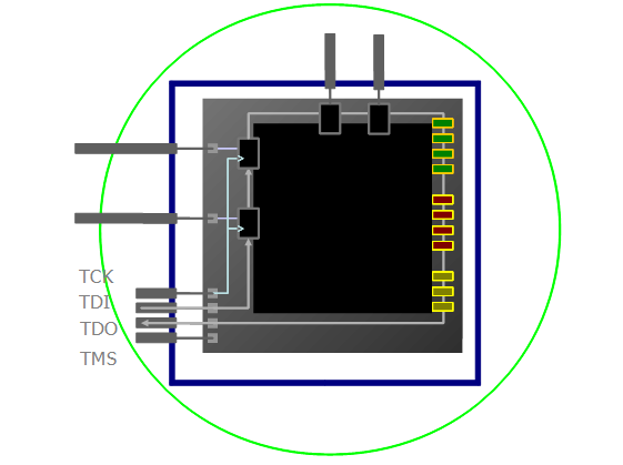
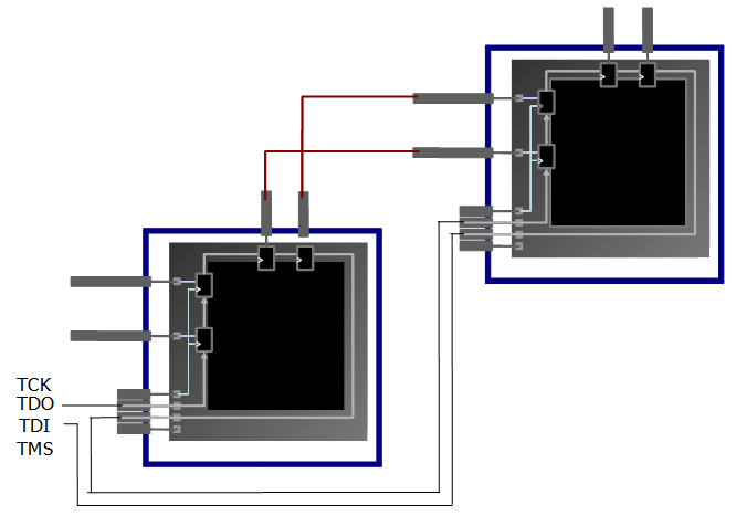
Test cells are inserted on the IC between the external pins. When Boundary SCAN mode is enabled, and the internal logic of the device is isolated from the pins and the test cells can output and read signals on the chips pins.
The TAP (Target Access Port)
The TAP or target access port is the interface to the on-chip Boundary SCAN test circuitry. The interface is comprised of 4 standard signals: TDI, TDO, TMS and TCK which allow access to the pins on the device is one long shift register. By clocking data into and out of the chip through this interface values at pins can be read and set to a logic one or zero.
Basic Tests with Boundary SCAN
 By setting pins on a Boundary SCAN enabled device to a high or low, and reading back the value from another device that is connected to the pin, basic tests can be accomplished.
Typically opens, shorts and stuck-at faults are detected using these simple techniques.
Boundary SCAN companies have created powerful tests that can be automatically generated based on how devices are connected and what each device can do.
Functional Test with Boundary SCAN
Boundary SCAN can be used to do functional tests on many devices such as: I2C and SPI based peripherals, RAM, DDR, FLASH and CPLDs and many others. Boundary SCAN companies include libraries for many popular devices that can be used to quickly test a device.
Functional and At-Speed Tests with Processor Emulation
Some Boundary SCAN tools support so called processor emulation mode for tests. This allows the tools to take control of a processor on a board and the load and run code. This technique allow you to run at speed (Burst Mode) RAM tests and high speed devices tests as well.
Functional and At-Speed Tests with Programmable Logic
Some tools allow programmable devices like CPLDs and FPGAs to be programed to perform tests in real time. This method can allow maximum speed programming of FLASH devices as well as at-speed tests on hardware accessible from the programmable device.
For More information please review our article on applications.
Comments on this entry are closed.
ssdcsdcd